
%20(1)%20wepb.webp "Verilog code for Basic NOT Gate")
Table of Contents
Basic of NOT Gate
Logic Symbol
%20(1)%20wepb.webp "Symbol of NOT Gate")
NOT gate has only one input signal and one output signal. The output state is always the opposite of the input state. It is also called as Inverters. The combination of Buffer and Not is NOT gate. Without the NOT it is called as Buffer. The Buffer processes the input information to output without any change.
Truth Table
| Input A | Output Y=A¯ |
|---|---|
| 0 | 1 |
| 1 | 0 |
- When the input A is 0, the output Y is 1.
- When the input A is 1, the output Y is 0.
This truth table shows the basic operation of a NOT gate, which inverts the input signal.
Boolean Equation
The Boolean equation for a NOT gate is a simple representation of its function. For an input A and output Y, the Boolean equation is:
Y=A¯
Here, A¯
denotes the logical NOT operation, indicating that the output Y is the inverse of the input A.
Timing Diagram
%20wepb.webp "Timing Diagram of NOT Gate")
Gate Level Modeling
Verilog Code in Gate-Level Modeling
module not_gate (
    input A,  // Input signal
    output Y  // Output signal
);

// Gate-level modeling of NOT gate
not (Y, A);

endmodule
Gate-level modeling of a NOT gate refers to describing its behavior and functionality using basic logic gates available in digital circuit design. In gate-level modeling, you specify how the gate operates at the lowest level of abstraction, which involves using predefined logic components like AND, OR, and NOT gates.
Data Flow Modeling
Dataflow modeling of a NOT gate, or any logic gate for that matter, describes its behavior in terms of how data flows through the circuit. Unlike gate-level modeling that focuses on the physical implementation using basic logic gates, dataflow modeling emphasizes the functional relationship between inputs and outputs.
The Boolean equation for a NOT gate is a simple representation of its function. For an input A and output Y, the Boolean equation is:
Y=A¯
Verilog Code in Dataflow modeling
module not_gate (
    input A,
    output Y
);

// Dataflow modeling using a NOT gate
assign Y = ~A;

endmodule
Behavioral Modeling
Behavioral modeling of a NOT gate, as well as any other logic gate or digital component, focuses on describing its functionality based on its intended behavior or operation, rather than specifying the implementation details or the flow of data through physical gates.
For Behavioral modeling, if you know the truth table of a logic, then you can easily design a logic using behavioral modeling.
Verilog Code in Behavioral Modeling
module not_gate (
    input A,
    output Y
);

// Behavioral modeling using an if-else statement
always @*
begin
    if (A == 0)
        Y = 1;
    else
        Y = 0;
end

endmodule
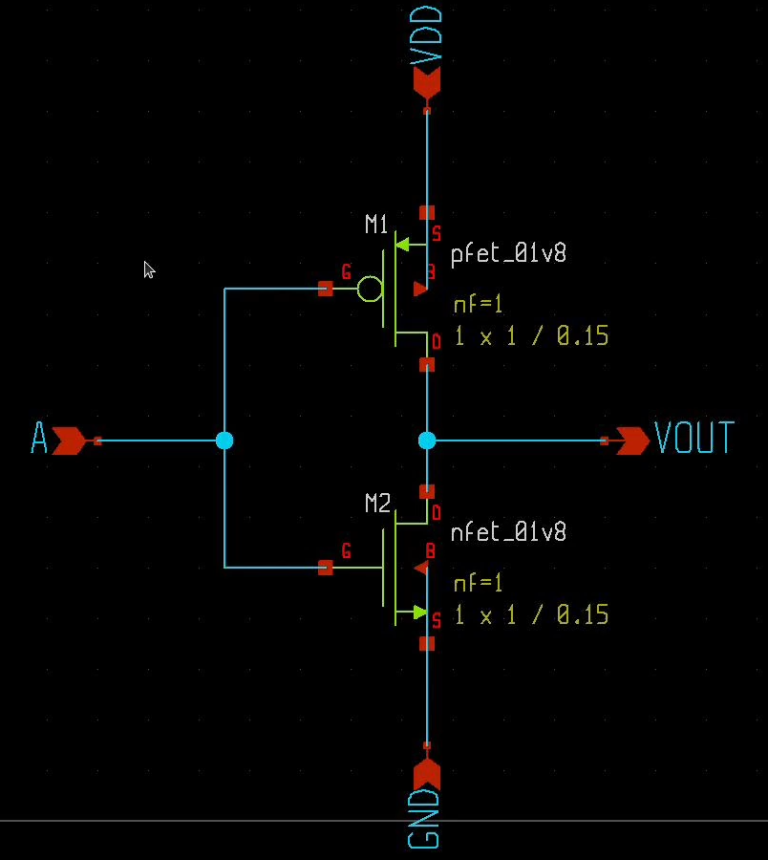
RTL Schematic of NOT Gate

- Input (A): The input labeled “A” represents a binary signal (either 0 or 1).
- Output (Not A): The output labeled “Not A” provides the logical negation of the input. If A is 0, then Not A is 1, and vice versa.
Functionality:
- When the input A is 0, the NOT gate allows current to flow through the path connected to “Not A,” resulting in a high output (1).
- Conversely, when A is 1, the NOT gate blocks current flow to “Not A,” resulting in a low output (0).
Testbench of NOT Gate
A testbench for a NOT gate is a Verilog module that is used to verify the functionality of the NOT gate module. It provides stimulus to the NOT gate module by applying inputs and observing the corresponding outputs.
`timescale 1ns / 1ps

module tb_not_gate;

  // Inputs
  reg A;

  // Outputs
  wire Y;

  // Instantiate the module under test (NOT gate)
  not_gate uut (
    .A(A),
    .Y(Y)
  );

  // Stimulus generation
  initial begin
    // Initialize inputs
    A = 0;

    // Apply input values and observe outputs
    // Test case 1: Input 0
    #10;  // Wait 10 time units
    A = 0;
    $display("Input A = %b, Output Y = %b", A, Y);

    // Test case 2: Input 1
    #10;  // Wait 10 time units
    A = 1;
    $display("Input A = %b, Output Y = %b", A, Y);

    // Add more test cases as needed

    // End simulation
    #10;  // Wait 10 time units before ending simulation
    $finish;
  end

endmodule
Waveform of the NOT Gate

Questions and Answers
Q: What is NOT gate formula?
A: The formula for a NOT gate is Y=A¯, where A is the input and Y is the output.
Q: What is the symbol for NOT gate?
A: The symbol for a NOT gate is a triangle with a small circle at its input.
Q: What is AND gate in Verilog?
A: In Verilog, an AND gate is described using the & operator. For example:
assign Y = A & B;
Q: What are the codes of logic gates?
A: The Verilog codes for basic logic gates are:
- AND gate:
assign Y = A & B; - OR gate:
assign Y = A | B; - NOT gate:
assign Y = ~A;
Q: How to use a NOT gate?
A: To use a NOT gate, apply the input signal to the gate’s input pin, and the output pin will provide the inverted output of the input signal.
Q: What is NOT gate truth value?
A: The truth table for a NOT gate is:
A | Y
-----
0 | 1
1 | 0
Q: Can a NOT gate have two inputs?
A: No, a NOT gate accepts only one input.
Q: What is the IC for NOT gate?
A: Common ICs (Integrated Circuits) for NOT gates include:
- 7404: Hex Inverter IC
- 74LS04: Low-Power Schottky Hex Inverter IC

[…] Verilog Code for Basic NOT Gate […]