
When p-type and n-type semiconductor materials are joined, a fascinating phenomenon occurs at their interface called as PN Junction and the diode is called PN Junction Diode, which I’d like to explain in detail.
Table of Contents
Introduction to PN Junction Diode
When a p-type semiconductor, rich in holes (positive charge carriers), is joined with an n-type semiconductor, which has an excess of electrons (negative charge carriers), they form what is known as a P-N junction. This junction is fundamental to many electronic devices, especially diodes.
Formation of the Depletion Region
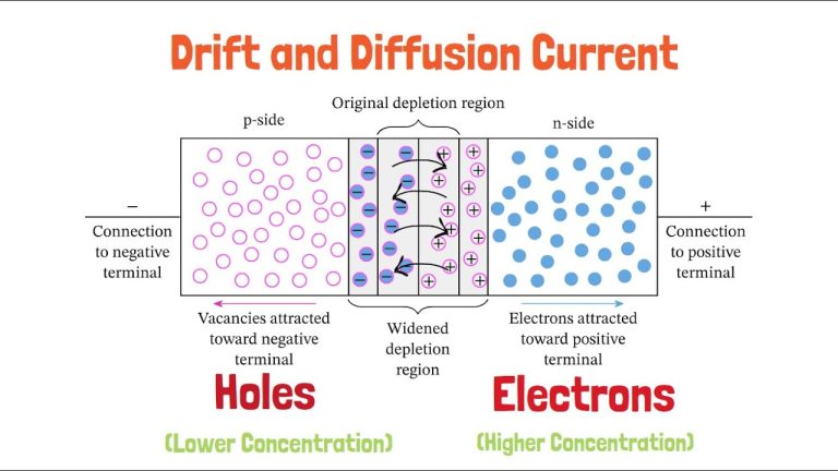
At the junction, electrons from the n-side diffuse into the p-side and recombine with holes there. Similarly, holes from the p-side diffuse into the n-side and recombine with electrons. This recombination leaves behind immobile ions: negative ions on the p-side and positive ions on the n-side. These ions create a region near the junction devoid of mobile charge carriers, called the depletion region or space charge region.
Potential Gradient and Barrier Formation
Because of the ions left behind, the p-side of the junction acquires a negative potential, while the n-side acquires a positive potential. This creates an electric field and a potential barrier across the junction. The negative potential on the p-side repels additional electrons trying to cross from the n-side, and the positive potential on the n-side repels holes trying to cross from the p-side. This potential barrier prevents further recombination and stabilizes the junction.
Role of Ions and Charge Carriers
The depletion region contains no mobile charge carriers-only fixed ions. The charge density is zero exactly at the junction but positive towards the n-type side and negative towards the p-type side. This region acts as an insulator, opposing the flow of majority carriers but allowing minority carriers to cross via drift current, which is caused by the electric field in the depletion region.
Width and Properties of the Depletion Region
The width of the depletion region depends on the doping levels of the semiconductors. Higher doping concentrations reduce the width of this region, roughly inversely proportional to the square root of the doping concentration. Typically, the depletion width is on the order of 0.5 micrometers, about the wavelength of visible light.
Electrical Behavior: Drift and Diffusion Currents
Initially, the diffusion of electrons and holes across the junction creates the potential barrier. The depletion region opposes the flow of majority carriers but assists minority carriers through drift current. This dual behavior makes the diode a bipolar device because current flow involves both electrons and holes.
Barrier Potential in Different Materials
The magnitude of the barrier potential depends on doping densities, electronic charge, and temperature. For common semiconductor materials, typical barrier potentials at room temperature (25°C) are about 0.3 volts for germanium and 0.7 volts for silicon.
Summary
In summary, the P-N junction forms a depletion region at the interface due to the recombination of electrons and holes, leaving behind charged ions that create a potential barrier. This barrier regulates charge carrier movement, enabling the diode’s rectifying behavior. The depletion region’s width and barrier potential depend on doping and material properties.
Questions & Answers
Q1: Why does the depletion region have no mobile charge carriers?
A1: Because electrons and holes recombine near the junction, leaving behind only immobile charged ions, which create the depletion region.
Q2: What causes the potential barrier in a P-N junction?
A2: The fixed ions on either side of the junction create an electric field and potential difference that oppose further diffusion of charge carriers.
Q3: How does doping affect the depletion region?
A3: Higher doping concentrations decrease the depletion width, as it is inversely proportional to the square root of doping density.
Q4: Why is the diode called a bipolar device?
A4: Because current flow involves both majority and minority carriers-electrons and holes-across the junction.
This explanation reflects my understanding of the P-N junction and its depletion region, based on semiconductor physics principles and verified sources.
Citations:
- https://www.pveducation.org/pvcdrom/pn-junctions/formation-of-a-pn-junction
- https://byjus.com/physics/p-n-junction/
- https://www.doubtnut.com/qna/113076647
- https://eng.libretexts.org/Bookshelves/Materials_Science/Supplemental_Modules_(Materials_Science)/Solar_Basics/D._P-N_Junction_Diodes/I._P-Type,_N-Type_Semiconductors
- https://www.youtube.com/watch?v=4SlfaocMfdA
- https://www.sigc.edu/sigc/department/physical/studymet/AnalogElectronicsStudyMaterial.pdf
- https://pubs.acs.org/doi/10.1021/cr900137k
- https://energyeducation.ca/encyclopedia/P-n_junction
- https://en.wikipedia.org/wiki/Depletion_region
- https://www.youtube.com/watch?v=6K358GINf6k
- https://www.wikiwand.com/en/articles/depletion_region
[…] law applies to both intrinsic and extrinsic (n-type and p-type) semiconductors, provided the material is not […]
[…] of clipping depends on diode […]