

In semiconductor physics, the movement of charge carriers—electrons and holes—is the cornerstone of modern electronic devices. Two fundamental processes govern this movement: drift and diffusion currents in semiconductors. These mechanisms are pivotal in the functionality of diodes, transistors, solar cells, and integrated circuits. This article delves into their principles, mathematical formulations, and practical implications, providing a comprehensive understanding essential for both students and engineers.
What Are Drift and Diffusion Currents?
Drift and diffusion currents are the primary means by which charge carriers propagate in semiconductors. Their interplay determines the electrical behavior of devices:
-
Drift Current: Caused by an external electric field, this current drives carriers (electrons and holes) in a directed motion.
-
Diffusion Current: Arises from spatial variations in carrier concentration, prompting carriers to migrate from regions of high density to low density.
The total current density in a semiconductor is the sum of these components:
Understanding their distinct roles is critical for analyzing phenomena such as p-n junction behavior and transistor operation.
Drift Current: Motion Under an Electric Field
When an electric field () is applied, carriers accelerate but frequently collide with lattice atoms, resulting in an average drift velocity ().
Key Equations
The drift current density for electrons and holes is:
Variables Explained:
-
: Elementary charge.
-
(cm⁻³): Electron and hole concentrations.
-
(cm²/V·s): Mobilities (e.g., Si: , ).
-
(V/cm): Applied electric field.
Factors Affecting Mobility
-
Temperature: Higher temperatures increase lattice vibrations, reducing mobility.
-
Doping: Impurity atoms scatter carriers, lowering mobility.
-
Material: GaAs has higher electron mobility () than Si, enabling faster devices.
Diffusion Current: Motion Due to Concentration Gradients
Carriers naturally diffuse from high-concentration to low-concentration regions, analogous to gas molecules spreading out.
Fick’s Law and Diffusion Coefficients
The diffusion current density is:
Variables Explained:
-
(cm²/s): Diffusion coefficients, linked to mobility via the Einstein Relation:
-
at room temperature.
Applications of Diffusion Current
-
p-n Junctions: Diffusion dominates in neutral regions, driving majority carriers across the junction.
-
Bipolar Transistors: Minority carrier diffusion across the base region determines current gain.
Drift vs. Diffusion: A Detailed Comparison
| Aspect | Drift Current | Diffusion Current |
|---|---|---|
| Driving Force | External electric field | Concentration gradient |
| Direction | Electrons: opposite to ; Holes: along | High → Low concentration (both carriers) |
| Governing Law | Ohm’s Law () | Fick’s Law () |
| Dependency | , , carrier density | , , material type |
| Typical Occurrence | Conductors, depletion regions | Non-uniform doping, illuminated semiconductors |
| Permittivity Role | Indirect (via ) | Independent |
Numerical Problems
Problem 1: Drift Current Calculation
Calculate the electron drift current density in silicon with , and .
Solution:
Problem 2: Diffusion Current Calculation
A silicon sample has a hole gradient and . Find .
Solution:
FAQs
Q1: Do drift and diffusion currents coexist?
Yes. In a p-n junction under bias, diffusion current dominates in neutral regions, while drift current prevails in the depletion zone.
Q2: How does temperature affect mobility and diffusion?
-
Mobility (): Decreases with temperature due to increased scattering.
-
Diffusion (): Increases slightly (since ), but carrier generation () dominates at high .
Q3: Why is the Einstein Relation significant?
It bridges drift and diffusion, showing they are interrelated manifestations of carrier motion under different forces.
Q4: Which current dominates in lightly doped vs. heavily doped regions?
-
Lightly doped: Diffusion (due to steeper concentration gradients).
-
Heavily doped: Drift (higher conductivity reduces needed for current).
Advanced Insights
Carrier Lifetime and Diffusion Length
The diffusion length (), where is carrier lifetime, determines how far carriers diffuse before recombining. This parameter is vital in solar cells and photodiodes.
High-Field Effects
At very high electric fields (), carriers gain enough energy to cause avalanche breakdown, a phenomenon critical in Zener diodes.
Conclusion
Drift and diffusion currents are foundational to semiconductor device physics. Mastery of these concepts enables the design of efficient electronic and optoelectronic devices, from nanoscale transistors to photovoltaic systems. Future explorations might delve into the continuity equation, which combines these currents with recombination processes, or Hall effect measurements for determining carrier mobility.

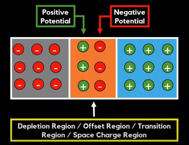
[…] The depletion region opposes the flow of majority carriers but assists minority carriers through drift current. This dual behavior makes the diode a bipolar device because current flow involves both electrons […]